Milestone Publications
Dissipationless zero energy epigraphene edge state for nanoelectronics
V. Prudkovskiy et al.,
Arxiv 1910.03697. [arXiv]
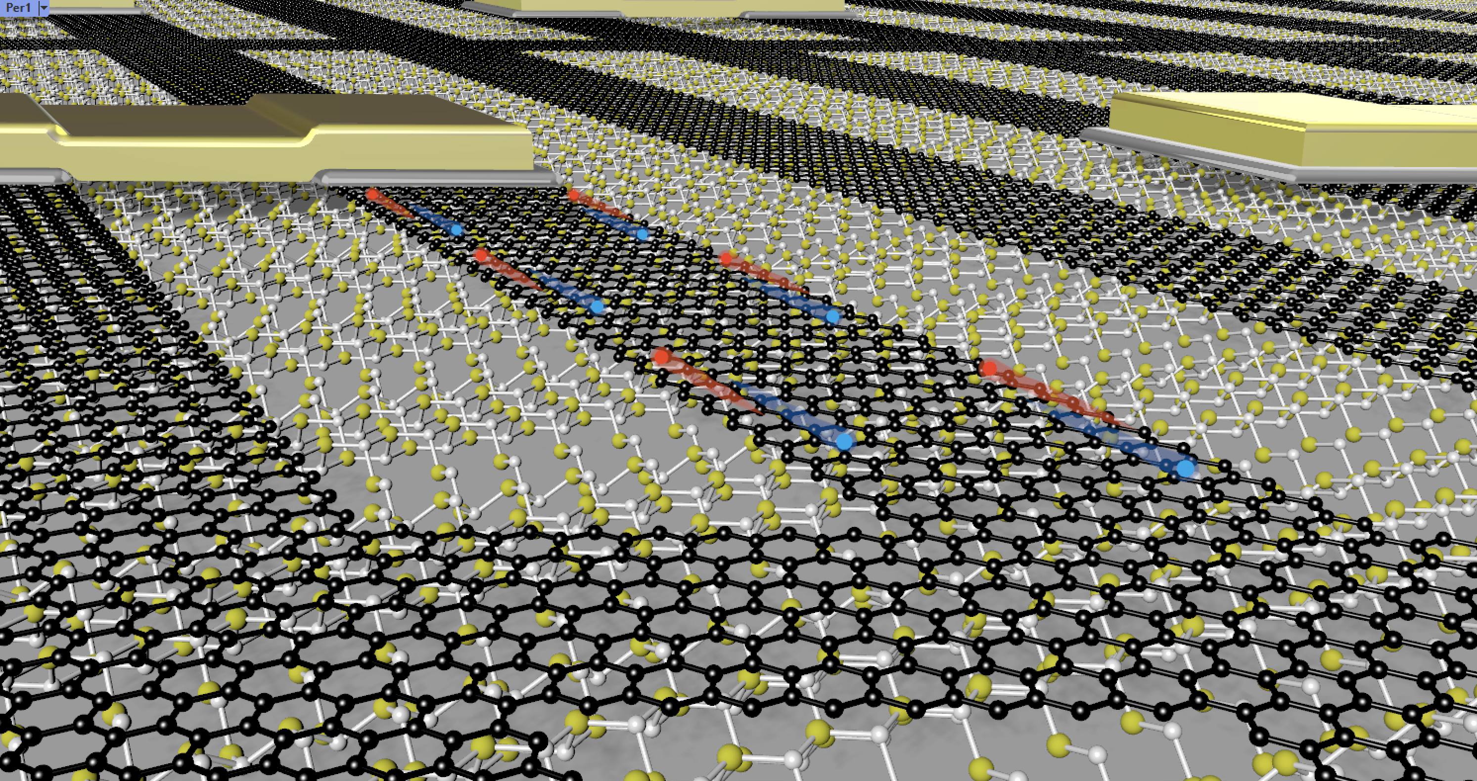
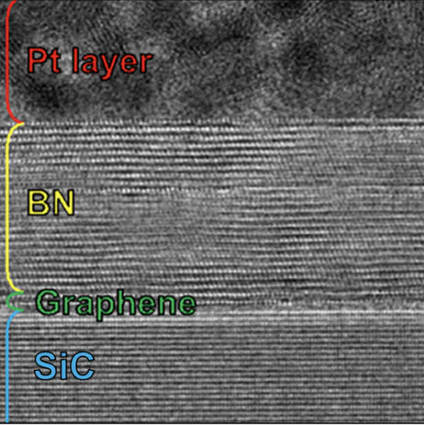
Highly Ordered Boron Nitride/Epigraphene Epitaxial Films on Silicon Carbide by Lateral Epitaxial Deposition
J. Gigliotti et al.,
ACS Nano 2020, 14, 12962. [arXiv]
Epigraphene, a review
C. Berger, E.H. Conrad, W. A. de Heer,
Landolt – Börstein encyclopedia Springer-Verlag GmbH Germany 2018, G. Chiarotti, P. Chiaradia (eds.), Physics of Solid Surfaces, Subvolume B, Chapter 166 (pp1-87). [arXiv]
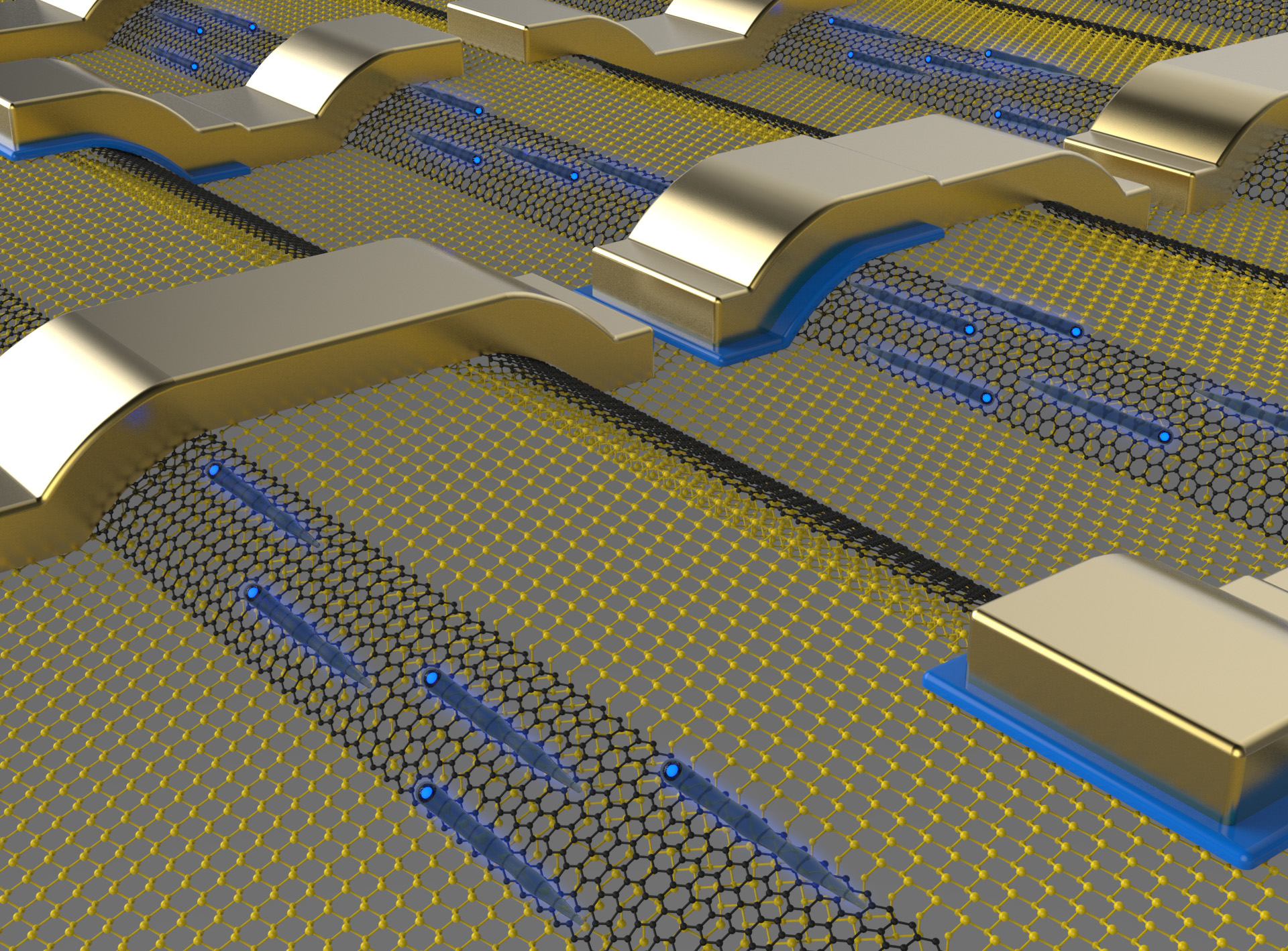
Exceptional ballistic transport in epitaxial graphene nanoribbons
J. Baringhaus et al.,
Nature, 506 (2014) 349. [arXiv]
Wafer bonding solution to epitaxial graphene-silicon integration
R. Dong, Z. Guo, M. Ruan, J. Kunc, S. K Bhattacharya, C. Berger, W. A. de Heer,
J. Phys D 47, 094001 (2014). [arXiv]
Record Maximum Oscillation Frequency in C-face Epitaxial Graphene transistors
Z. Guo, R. Dong, P.S. Chakraborty, N. Lourenco, J. Palmer, Y. Hu, M. Ruan, J. Hankinson, J. Kunc, J. D. Cressler, C. Berger, W. A. de Heer,
Nano Letters 13, 942 (2013). [arXiv]
Large area and structured epitaxial graphene produced by confinement controlled sublimation of silicon carbide
W. A. de Heer, C. Berger, M. Ruan, M. Sprinkle, X. Li, Yike Hu, B. Zhang, J. Hankinson, E.H. Conrad,
PNAS 108 (41) 16900 (2011). [arXiv]
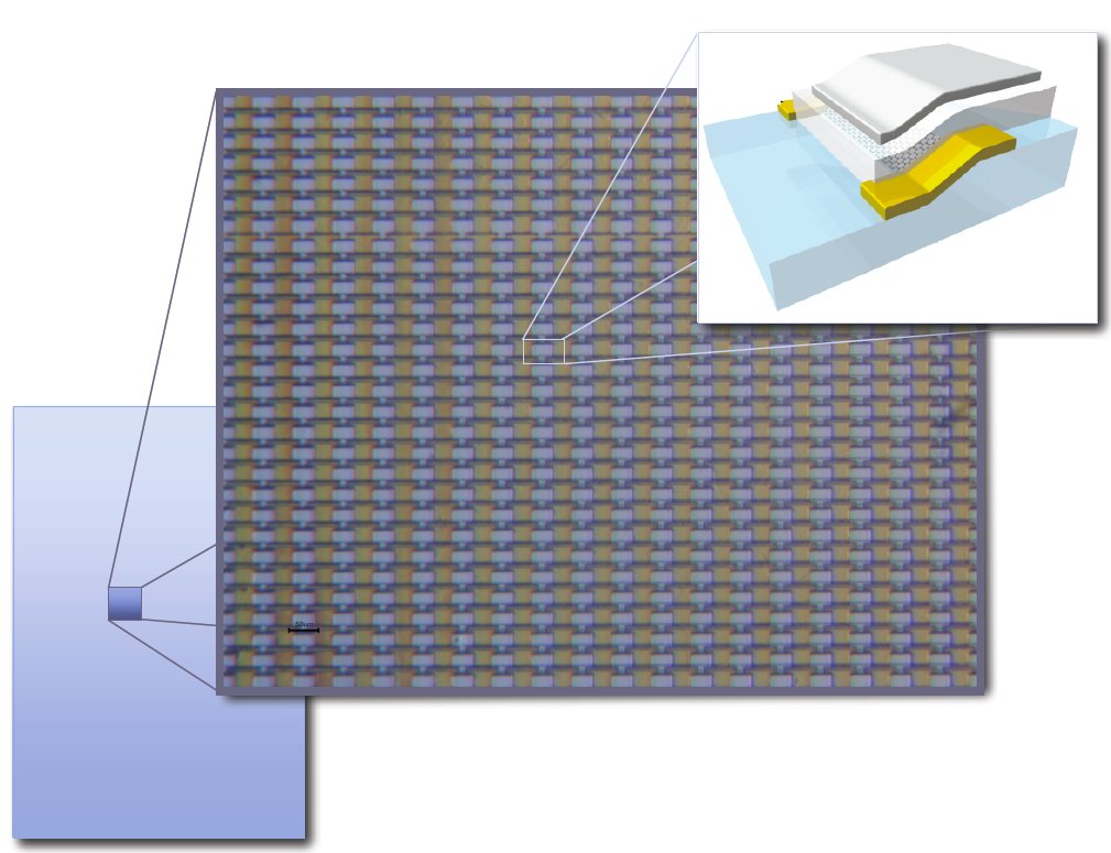
Scalable Templated growth of graphene nanoribbons on SiC
M. Sprinkle, M. Ruan, X. Wu, Y. Hu, M. Rubio-Roy, J. Hankinson, C. Berger, W. A. de Heer,
Nature Nanotechnology 5, 727 (2010). [arXiv]
Half integer quantum Hall effect in high mobility single layer epitaxial graphene
X. Wu, Y. Hu, M. Ruan, N. K. Madiomanana, J. Hankinson, M. Sprinkle, C. Berger, W. A. de Heer,
Applied Physics Letters 95, 223108 (2009). [arXiv]
First direct observation of a nearly ideal graphene band structure
M. Sprinkle, D. Siegel, Y. Hu, J. Hicks, P. Soukiassan, A. Tejeda, A. Taleb-Ibrahimi, P. Le Févre, F. Bertran, S. Vizzini, H. Enriquez, S. Chiang, C. Berger, W. A. de Heer, A. Lanzara, E. H. Conrad,
Phys Rev Lett 103, 226803 (2009). [arXiv]
Epitaxial Graphene Electron Devices on SiC Substrates
J. Kedzierski, P.-L. Hsu, P. Healey, P. Wyatt, C. Keast, M. Sprinkle, C. Berger, W. A. de Heer,
IEEE Transactions on Electron Devices 55, 2078 (2008). [arXiv]
Why Multilayer Graphene on 4H-SiC(000-1) Behaves Like a Single Sheet of Graphene
J. Hass, F. Varchon, J. E. Millan-Otoya, M. Sprinkle, W. A. de Heer, C. Berger, P. N. First, L. Magaud, E. H. Conrad,
Phys. Rev. Let 100, 125504 (2008). [HAL]
Landau level-spectroscopy of ultra-thin graphite layers
M. Sadowski, G. Martinez, M. Potemski, C. Berger, W.A. de Heer,
Physical Review Letters 97, 266,605 (2006). [arXiv]
Electronic confinement and coherence in patterned epitaxial graphene
C. Berger et al.,
Science, 312 (2006) 1191-1196. [Link]
Ultrathin Epitaxial Graphite: 2D Electron Gas Properties and a Route Toward Graphene-Based Nanoelectronics
C. Berger et al.,
J Phys Chem B, 108 (2004) 19912-19916. [arXiv]